Copyright © 2002-2005, 2008, 2024 Kees Krijnen.
PCB Etching
Since the introduction of laser printers making your own PCBs (Printed Circuit Boards) has become fairly easy. The method described here assumes you want to make a PCB from an electronics magazine PCB layout - so you can copy it with a copier - or you are able to print your own PCB layouts from a PCB design package or have them available in electronic format and you can print them with a laser printer.
I am using the described method below successfully since 1996. I was forced to find an etching method to be used at home after the company I worked for dumped their prototype PCB production tools. A short version of the `greasy' etching method has been published August 2000 in the newsletter `Vijgeblaadje' from the Dutch FIG (HCC Forth gebruikersgroep).
- PCB Layout
- PCB Preparation
- PCB UV Exposure
- PCB Development
- PCB Etching
- Trouble shooting
- More Examples
PCB Layout
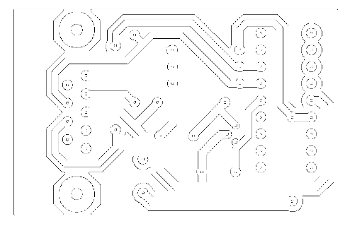
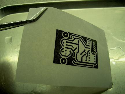
The PCB layout is a mirrored positive one - black on white. Mirrored as viewed from the silkscreen top (component) side. The PCB layout is printed 1:1 on paper by means of a laser printer or copier machine. The laser printer or copier toner will not run out when it gets wet or oily. The ink of an inkjet paper print does run out and inkjet printers are therefore useless with the described method.
I have used several types of HP laser printers (LaserJet Series II, 5L, 4000 and 1100). These printers work fine. It might be possible that the toner texture on the layout prints from your used laser printer is not dense enough and passes too much light. However, results might be improved by setting the toner density to maximum. Generally printer driver properties allow to set the toner density.
|
Positive mirrored (top view) layout |
|
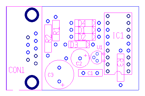
Component (top view) layout |
PCB Preparation
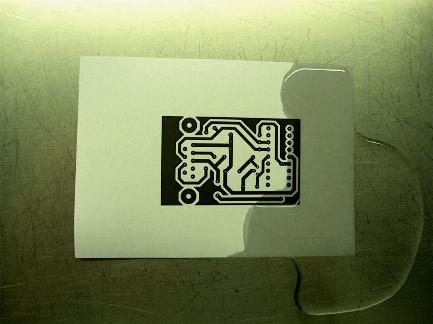
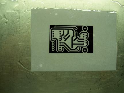
The PCB layout paper is drenched with sunflower seed oil. Sunflower seed oil is common available from your local grocery or wall market. Superfluous oil should be removed carefully with tissue paper. The sunflower seed oil is used to make the white part of the layout paper transparent for light.
If you prefer to use the PCB layout more than once let the drenched PCB layout paper dry at least 48 hours. The layout paper should be carefully dried on forehand as much as possible with tissue paper. Sunflower seed oil is a `drying' oil. Exposed to the air over a number of hours, the layout paper becomes rigid again. A kind of polymerization takes place. You will get a lot less or no greasy fingers anymore afterwards.
Other mineral or vegetable oils might work as well to obtain light transparency. However, they might not be `drying' oils. When I started experimenting, sunflower seed oil was the first oil I used and it worked fine. So I didn't try any other oils. Using water does not work. The layout paper crumples up a bit.
|
Drench layout with sunflower seed oil |
Layout fully drenched |
|
Greasy layout |
PCB UV Exposure
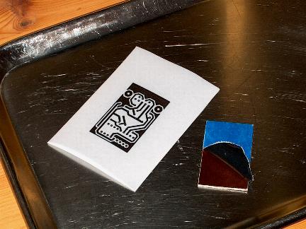
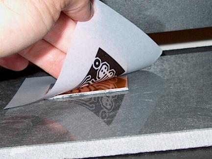
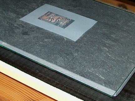
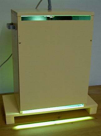
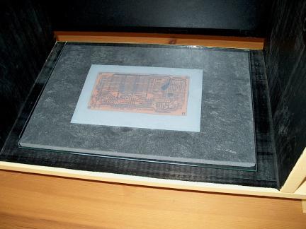
The protective plastic layer is removed - peeled back - from the photosensitive PCB. The toner side of the greased layout is placed on the copper of the PCB. Captured air-bubbles are gently pressed away from underneath the layout. The PCB with the layout is now covered with an appropriate sized windowpane and placed on a piece of plain polished tile or marble. The tile or marble absorbs the heat coming from the UV bulb, which is significant. Three to four minutes 300W bulb UV exposure from a distance of 30-40 cm will do the photo process. Take care when finished and removing the PCB, it gets hot!
|
Home-built UV exposure box with 300W UV bulb, polished tile and window pane |
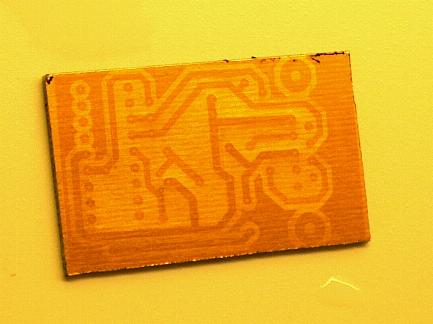
PCB with partly peeled back protective plastic layer and `dried' layout |
|
Place layout with toner side on copper of the PCB |
Cover PCB and layout with window-pane |
|
Exposure |
PCB Development
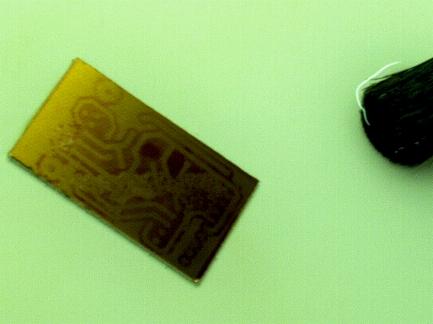
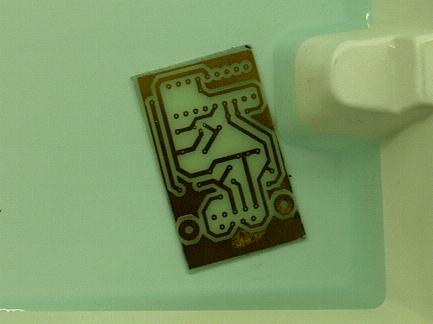
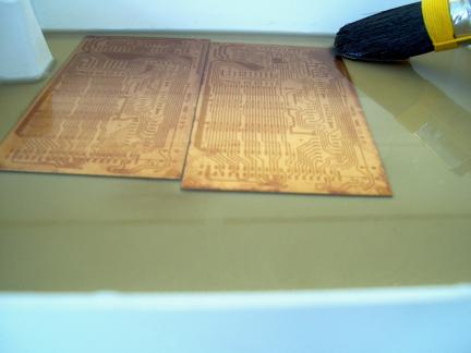
The PCB is developed with a 1% solution of sodium hydroxide NaOH. You can make this solvent by adding 10 gram of sodium hydroxide pellets to 1 liter of water and mix it until everything is dissolved. Use a brush to speed up the developing and clean the PCB during this process if the PCB is still greasy due to the applied sunflower seed oil. The developing process takes about 1 minute. It is sometimes difficult to guess when the developing is finished. The traces should become clear and the exposed photosensitive layer has dissolved (during the brushing you see darker `cloud' coming off the PCB surface).
|
Gently brush the PCB |
Almost developed, some traces are not clear yet |
PCB Etching
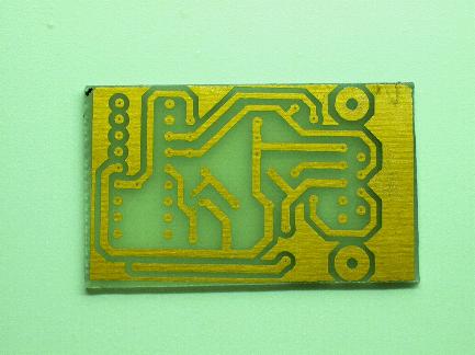
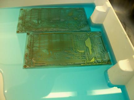
The developed PCB is etched with a 220 g/l solution of ammonium peroxydisulfate (NH4)2S2O8 a.k.a. ammonium persulfate, 220 gram added to 1 liter of water and mix it until everything is dissolved. Theoretically it should be possible to etch slightly more than 60 grams of copper with 1 liter etching solution. Assume an 50% efficiency, about 30 grams of copper. With a thickness of 35 µm copper on your PCB this covers a copper area of about 1000 cm2. Unfortunately the efficiency of the etching solution degrades, dissolved ammonium peroxydisulfate decomposes slowly. You better make just enough etching solution you need to etch. For an etching tray of about 20 x 25 cm a minimum practical amount is 200-250 ml solution. So you dissolve about 44 grams ammonium peroxydisulfate into 200 ml or 55 grams into 250 ml water.
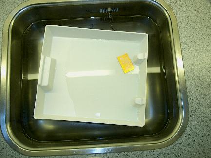
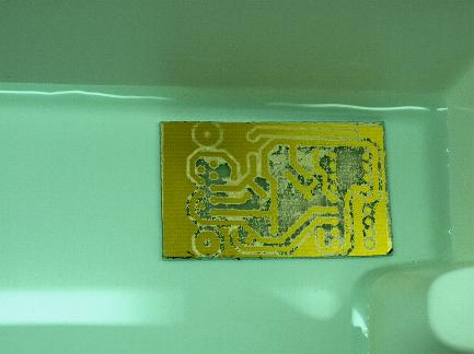
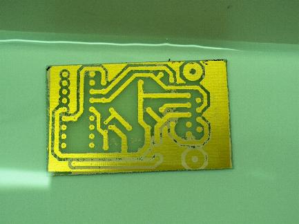
Etching at ambient temperature might take over an hour, it is better to heat up the etching solvent to about 35-45 degrees Celcius. The etching solution heating up could be done in a microwave oven, this takes about 40 to 60 seconds in a 850W microwave oven depending on the initial temperature of the etching solution (hint: first try this with just water to determine the timer setting of the microwave oven). The etching - rocking the etching tray - takes about 15-30 minutes at this temperature. If you have a heated, air-bubble circulated etching fluid tank available, this is probably the fastest way to etch. At higher temperatures the etching performance decreases. The etching process is an exothermic reaction, it generates heat. Take care, cool your etching tray when necessary! You should minimize the amount of copper to etch by creating copper area in your PCB layout as much as possible. When starting the etching process and little to etch it is difficult to keep the etching solution at 35-45 degrees Celcius. It helps to fill for example the kitchen sink with warm water and rock the etching tray in the filled kitchen sink.
When the ammonium peroxydisulfate is dissolved it is a clear liquid. After an etching procedure it gradually becomes blue and more deeper blue - the chemical reaction creates dissolved copper sulfate CuSO4. Compared to other etching chemicals like hydrated iron (III) chloride FeCl3.6H2O a.k.a. ferric chloride or the combination of hydrochloric acid HCL and hydrogen peroxide H2O2, using ammonium peroxydisulfate is a clean and safe method. Did you ever spilled dissolved iron chloride on your clothes or your assumed stainless steel kitchen sink? Do you really want to keep concentrated hydrochloric acid and hydrogen peroxide at home? So, without doubt ammonium peroxydisulfate is the best choice for etching at home. However, copper sulfate is a poisonous substance and should be treated as chemical waste.
|
Rock the etching tray |
The epoxy of the PCB becomes visible |
|
Almost finished |
The etching solution colors slighty blue |
|
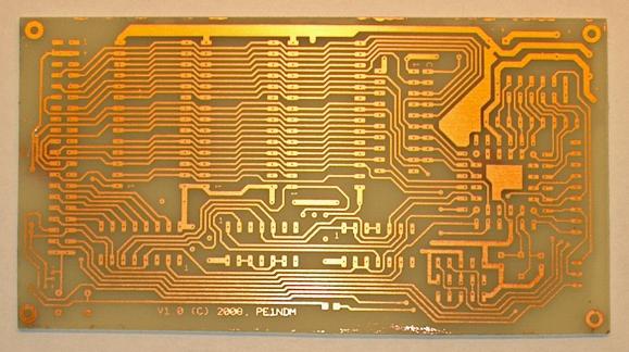
Finished |
Trouble shooting
The above mentioned exposure timing should be determined experimentally. But even when the exposure timing is correct PCB etching failures could happen because of low quality or too old photosensitive PCB, the photosensitive layer has aged despite the protective plastic layer. Other possible causes are too high concentration of development solution causing the photosensitive part not exposed to light to be dissolved by the sodium hydroxide solution as well. When developing too short not all of the copper of the PCB will be etched. Developing might take some experimenting to get used to it and know what to expect. Furthermore set the toner density of your laser printer driver always to maximum.
More examples
|
Exposure |
Development |
|
Etching |
|
Finished |

